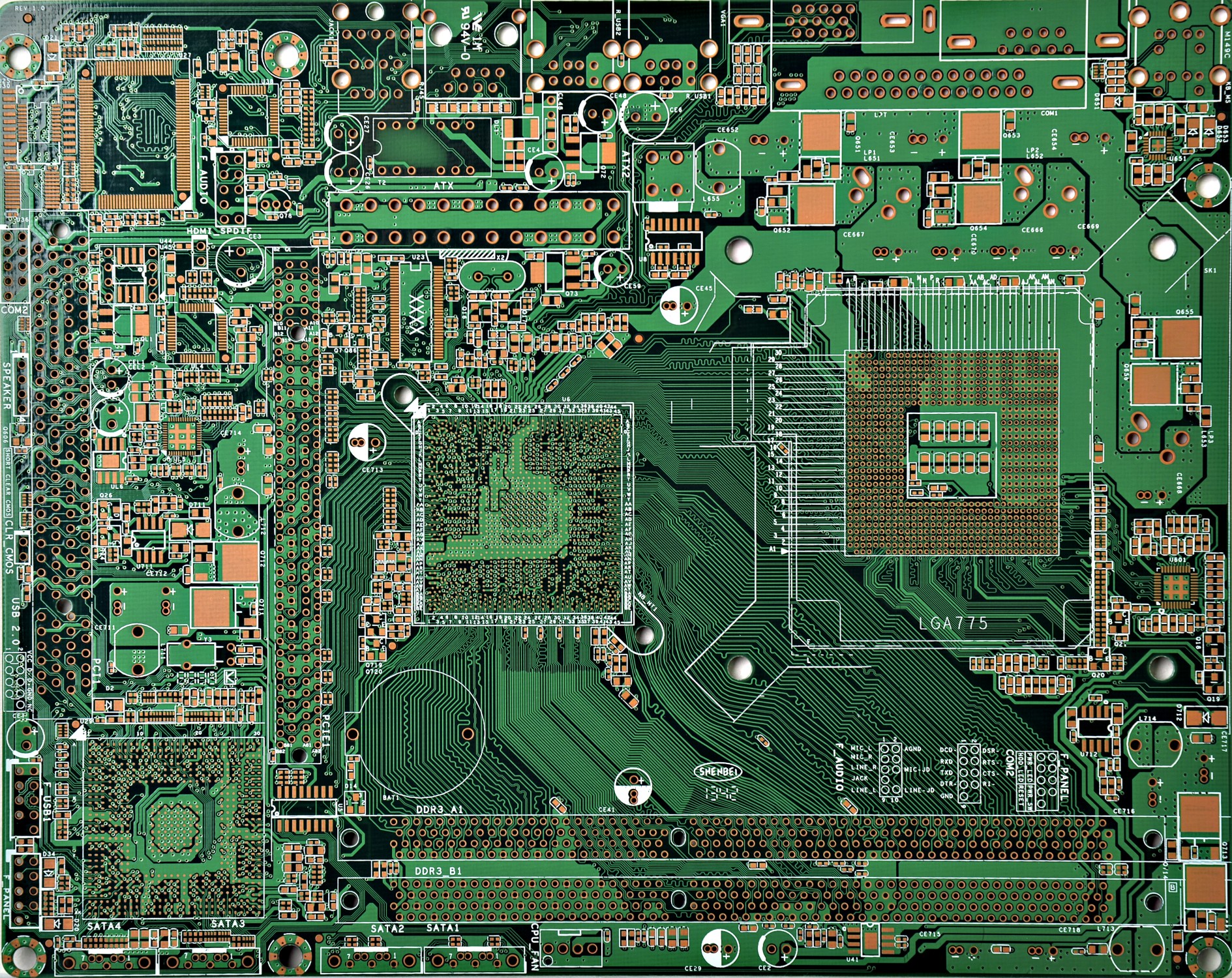
Comparison of LDI and CCD Exposure Systems
Comparison Between LDI and CCD Exposure Machines
Before analyzing the reasons behind LDI’s slower exposure speed, let’s first compare the differences between LDI (Laser Direct Imaging) and traditional CCD exposure machines.
LDI (Laser Direct Imaging)
LDI is an advanced exposure technology that uses lasers to directly image circuit patterns onto PCBs without requiring physical photomasks. Its advantages include:
-
Eliminates photomask production, reducing material and processing costs.
-
Higher precision in alignment, minimizing registration errors.
-
Shorter lead times for prototypes and improved production flexibility.
CCD Exposure Machines
Traditional CCD semi-automatic exposure machines rely on photomasks to transfer circuit patterns onto PCBs. While this method has been the industry standard for years, it has limitations:
-
Photomask production and handling increase costs and time.
-
Alignment errors may occur, affecting accuracy.
-
Lower efficiency compared to maskless technologies.
Factors Affecting LDI Exposure Speed
To understand why LDI exposure is slower, we must examine the key factors influencing its speed:
-
Energy Density:
-
Photoresist requires sufficient energy for proper exposure. High-sensitivity photoresist reduces exposure time, but energy density depends on the light source design.
-
-
Data Modulation Speed:
-
The laser’s modulation rate determines the number of light points drawn per second. Higher resolution demands increase exposure workload.
-
-
Mechanical Movement Speed:
-
The PCB’s movement during exposure (e.g., acceleration/deceleration mechanisms) directly impacts throughput.
-
Why Is LDI Exposure Slower?
The slower speed of LDI stems from the interplay of the above factors:
-
High-quality exposure requires adequate energy delivery, which takes time.
-
Mechanical limitations (e.g., stage movement precision) prioritize accuracy over speed.
Despite this, LDI excels in high-precision PCB fabrication, especially for prototypes, offering unmatched accuracy and eliminating photomask costs. However, for mass production, its slower speed remains a bottleneck, prompting some manufacturers to retain CCD machines for high-volume tasks.
Advancing Toward More Precise and Complex PCB Manufacturing

High-Density Interconnect (HDI) PCBs
High-Density Interconnect (HDI) PCBs are commonly used to interconnect various components in compact, miniaturized packages. They incorporate micro-feature technologies to enhance electrical performance. These boards feature a reduced form factor, making them ideal for shrinking component sizes. Beyond minimizing PCB dimensions, this design characteristic also improves the performance of electrical systems.

Applications of HDI PCBs
HDI PCBs are widely adopted in advanced technological products, such as:
-
High-speed chips
-
Multi-pin-count components
-
Fine-pitch devices
Thanks to their design attributes—including ultra-fine line widths, laser-drilled microvias, multiple lamination cycles, and high-frequency materials—these PCBs deliver diverse functionalities within a limited unit area. By incorporating stacked laser-drilled microvias, they ensure critical signal integrity and routing solutions for demanding modern applications.
Advantages of HDI Technology
HDI PCBs leverage cutting-edge technologies to optimize functionality and signal integrity. Their design enables enhanced performance within the same or even smaller spatial footprint. The rapid evolution of PCB manufacturing technologies has driven innovations aligned with societal demands, including:
-
5G communication systems
-
Wearable medical devices
-
Autonomous vehicles
Key Features of HDI PCBs
-
Microvia Technology: Laser-drilled microvias enable dense interconnections.
-
Fine Line/Space: Supports ultra-narrow traces (e.g., ≤ 75μm).
-
Advanced Materials: High-speed laminates minimize signal loss.
-
Sequential Lamination: Ensures reliability in multi-layer designs.
FAQ
-
Is LDI unsuitable for mass production due to its slower speed?
Yes. LDI is ideal for prototypes and small batches but less efficient for large-scale production. -
Which is more precise: LDI or CCD?
LDI is more precise. Direct imaging reduces alignment errors and enhances pattern fidelity. -
How does LDI reduce costs?
Eliminates photomask expenses and accelerates prototyping, lowering overall development costs.
Conclusion
LDI technology revolutionizes PCB manufacturing with precision and flexibility, though its slower speed limits its use in high-volume scenarios. Understanding these trade-offs helps manufacturers strategically adopt LDI for prototyping while leveraging CCD for mass production.
For further details on PCB manufacturing or LDI technology, feel free to contact me –Meidear PCB mailto mkt@me-pcb.com


(Reporting Live from Guangya Expo 2025)

CEM-3 Thermal conductive material
IMS pcb Flexible pcb Copper-base pcbs

HASL,OSP ENIG,Immersion Silver,Immersion Tin hard Gold
nickel P-alladium gold

